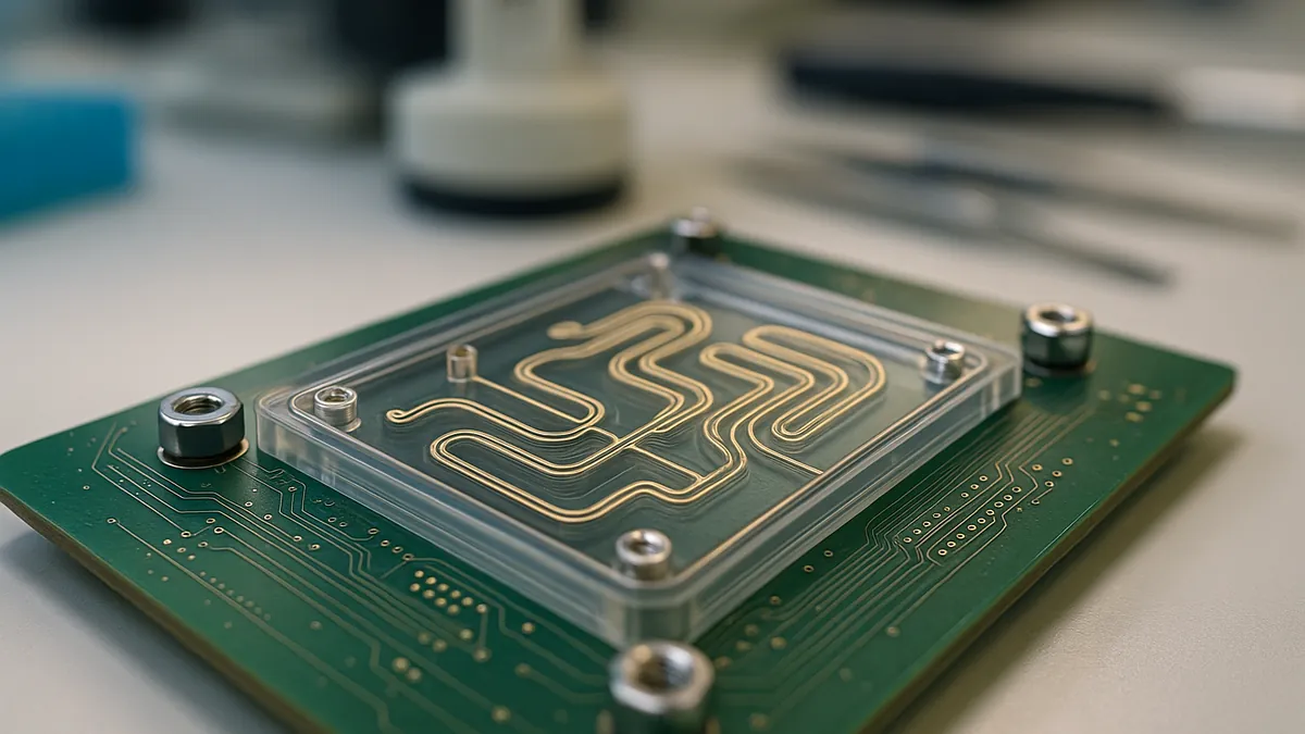
Lab-on-a-chip is still not a turnkey platform for mass deployment, but one signal is becoming hard to miss: commercialization work is moving toward Lab-on-PCB designs because they use established printed circuit board manufacturing to cut cost and combine electronics with microfluidics in a way that academic prototypes often do not. That shift matters less as a branding change than as a manufacturing checkpoint for whether point-of-care devices can be produced repeatedly, affordably, and at useful scale.
Why PCB manufacturing is now central to the field
For years, Lab-On-a-Chip research showed what miniaturized diagnostics could do in controlled settings, but fabrication choices often kept systems stuck at prototype stage. Lab-on-PCB changes the emphasis by building around a supply chain that already knows how to produce fine features, multilayer interconnects, sensors, and control electronics at industrial volume. In practical terms, that gives developers a more direct route to integrating fluid handling, signal processing, and readout on one platform than custom silicon, glass, or one-off polymer builds usually allow.
This does not mean PCB is automatically the best substrate for every assay. It means the industry is increasingly testing a more realistic commercialization path: start with a process that already has standardization, manufacturing partners, and known cost curves, then adapt microfluidic functions around it. For clinical and point-of-care products, that can matter as much as assay performance because deployment depends on whether devices can be assembled, calibrated, and replaced without boutique fabrication.
Materials are deciding what can leave the lab

Material choice is still one of the biggest filters between a convincing demo and a product. Silicon and glass offer strong technical properties, including semiconducting behavior and optical transparency, but they are expensive and rigid, which limits design freedom and raises integration costs. PDMS and related polymers are easier for prototyping, more flexible, and often friendlier for early microfluidic experiments, yet the soft-lithography workflows behind them do not translate cleanly into high-volume production.
The trade-offs become clearer when fabrication method is tied to business reality rather than lab convenience. Injection molding can support high-volume LoC production once a design stabilizes, but the tooling cost is high enough to punish frequent iteration. 3D printing does the opposite: it reduces turnaround time for prototypes and custom geometries, but it is still poorly suited to mass manufacturing when consistency, throughput, and unit economics become the priority. That is why standardized scalable processes, not just clever chip designs, are the next checkpoint for the field.
| Platform or method | Main advantage | Main limit | Best fit today |
|---|---|---|---|
| Silicon / glass | High-performance material properties | Costly, rigid, harder to scale into flexible integrated products | Specialized devices, research systems |
| PDMS and similar polymers | Fast prototyping, flexibility, gas permeability | Soft-lithography scalability limits | Early-stage design and testing |
| Injection molding | Strong for volume production | High upfront tooling cost | Mature product lines with stable designs |
| 3D printing | Rapid iteration and custom geometries | Not ideal for mass production consistency and scale | Prototype development |
| Lab-on-PCB | Uses standardized PCB manufacturing and easier electronics integration | Still needs application-specific fluidic and fabrication optimization | Commercialization-focused integrated platforms |
Flow control and detection are where portability often breaks down
LoC systems are not defined only by chip material. They also depend on how samples move and how signals are detected. Centrifugal systems support modular disposable cartridges and are attractive for assay packaging, but the need to rotate the platform complicates portability and makes it harder to integrate actuation and sensing in the same operating state. Electrokinetic approaches such as dielectrophoresis and electrowetting-on-dielectric allow precise manipulation of particles and droplets, yet that precision comes with more complex electrode fabrication and stronger dependence on advanced detection hardware.
Detection choice then reshapes the whole device. Lateral flow assays remain dominant in point-of-care settings because they are cheap and simple, but their sensitivity is lower than nucleic acid amplification tests. NAAT-based systems are gaining interest because they can deliver faster and more sensitive pathogen detection, including use cases such as infectious disease diagnosis and viral load monitoring, but they also raise integration demands around thermal control, signal quality, and power. Miniaturization does not remove those burdens; it can worsen signal-to-noise constraints and force more careful engineering of the readout chain.
Digital microfluidics and paper devices show the split in deployment goals
Two active branches of the field point in different commercial directions. Digital microfluidics uses microelectrode arrays to move discrete droplets, which can reduce reagent use, lower contamination risk, and support parallel operations. The catch is that droplet behavior varies with sample properties, and portable systems still need to be robust enough to handle that variability outside controlled lab conditions.
Paper-based LoC devices target the opposite end of the market: very low-cost testing for resource-limited settings. That improves accessibility, but paper formats still struggle with multiplexing and deeper functional integration. In other words, lower cost alone does not solve the same problem that Lab-on-PCB is trying to solve. One path pushes affordability at the edge of functionality; the other tries to preserve more integrated capability while using a manufacturable electronics platform.
The next checkpoint is process standardization, not bigger promises
The near-term question is not whether Lab-On-a-Chip can produce impressive results; research has already shown that repeatedly. The harder test is whether developers can settle on fabrication processes that balance cost, resolution, and design flexibility across different applications without rebuilding the production stack each time. That is the variable most likely to determine whether clinical, bedside, and home-use systems move beyond pilot deployments in the next few years.
That also sets a practical filter for buyers, partners, and regulators. If a platform still depends on bespoke fabrication, external control hardware, or fragile detection conditions, it is not yet a mass-market product no matter how compact the chip appears. The more credible candidates are the ones that can show repeatable manufacturing, integrated electronics, and a clear path from prototype method to production method. Right now, Lab-on-PCB is attracting attention because it addresses that deployment reality more directly than many earlier LoC architectures.